Application of Strobe Application Devices
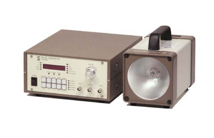
Strobe Application Devices are used in various applications. As the stroboscopes, they are used in universities and laboratories for research and study, and in the industry they are high-end light sources of the automated optical inspection (AOI) system.
As the heat source, they have been put to use in the thermophysical testing devices and IR non-destructive testing devices in the measuring fields, and in the industry they have been used as the heat source for annealing silicon wafer of semiconductors, as the solar simulators to test I-V characteristics of solar cells, and recently as the heat source for burning the nano-metal ink in the printed electronics field.
-
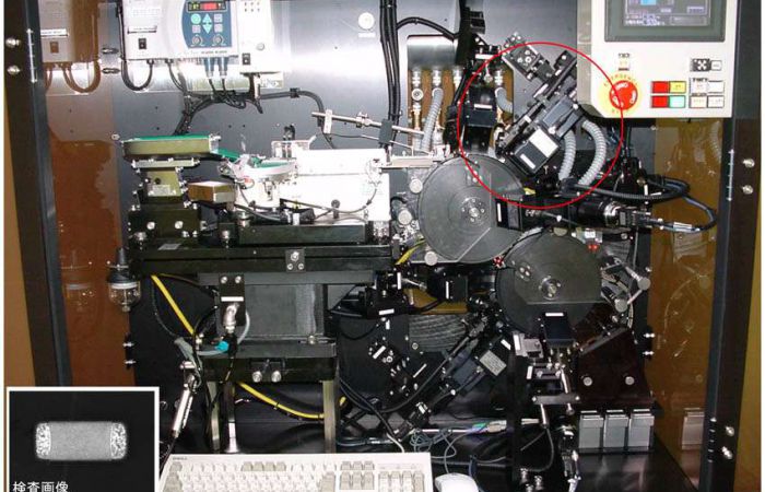
Chip external inspection system
Deploying strobe light sources and cameras installed at 6 locations and linked by coaxial fibers, these systems capture images of passing microscopic chips at high speed to determine product acceptability (at rates up to 1,200 pieces per minute).
-
Shape estimates using dual light source photometric stereo
Making active use of multiple light sources for image shape evaluations, current research targets methods for determining the orientation and shape of objects based on differences in the brightness detected when surfaces are illuminated by strobe light sources from various directions. In one example, this method can be applied to measure the size of an affected area, a task that would normally be difficult to determine through an endoscope, thereby increasing the reliability and safety of medical diagnoses. This method also promises various benefits in industrial and disaster rescue applications.
-
Semiconductor lifetime measurement
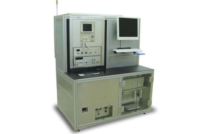
For various silicon wafer processing and device manufacturing processes, measurements of carrier lifetimes* are growing increasingly important in research and analysis related to metallic contamination and crystal defects. The silicon ingot lifetime measurement system manufactured by Napson Corporation incorporates Sugawara strobes to ensure consistent lifetime measurement meeting rigorous measurement standards.
-
Observation of speaker cone vibrations
To produce high-quality sounds, the speaker cone of an audio loudspeaker must vibrate in a manner faithful to the audio signals supplied. With a Stroboscope, we can examine high-speed vibrations of the speaker cone when driven by an audio signal and observe them directly in slow motion with the naked eye.*
-
Observing the airborne state of ink for an inkjet printer
Sugawara nano pulse lights are widely used in laboratories to observe and photograph the airborne state of ink for inkjet printers.
-
Acoustic wave research
Sugawara nano pulse lights are used in research to visualize acoustic wavefronts in various phenomena attributable to sound waves and ultrasound in the 10 kHz to 100 kHz band for applications in medical field and other fields.
-
Semiconductor exposure system
Sugawara nano pulse lights are used to observe sprays of target substances (such as liquid xenon) illuminated with laser light in a state-of-the-art semiconductor exposure system incorporating a laser-excited plasma light source.
-
Observing behavior of cation radicals in organic substances
Sugawara nano pulse lights are used as light sources to observe the behavior of cation radicals (positive ions) generated in organic substances excited by laser light.
-
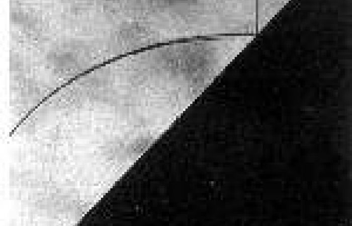
Research on reflected waves generated when supersonic impulse waves propagating within a compressible fluid strike inclined planes
Sugawara nano pulse lights are used as light sources in research involving the Schlieren method to observe reflected waves generated.
Example: Visualizing an impulse wave striking and reflection normally against an inclined plane. -
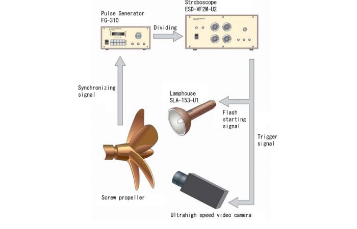
Observation of cavitation caused by the screw propeller
When the screw propeller of a ship operates underwater, a swirling effect called cavitation occurs. This swirling effect is closely related to the ship's propulsive efficiency as well as propeller cracking and damage. As such, cavitation has been a topic of detailed research for many years.
